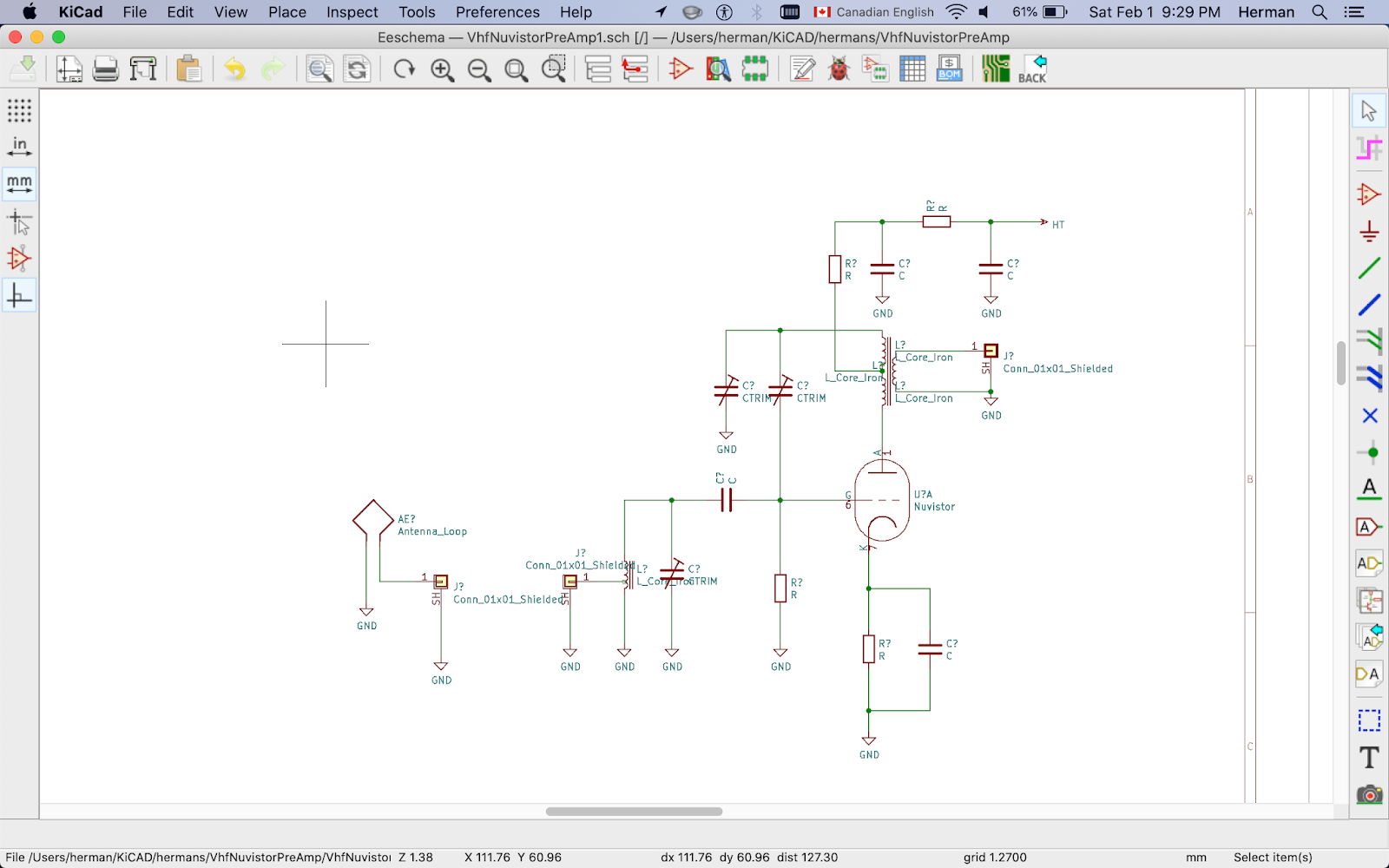
Kicad 5 schematic to pcb Kicad schematic text color and block diagram Kicad circuit connection elements between schema ed info 1080 1920 kb
Move block in schematics - Schematic - KiCad.info Forums
Kicad schematics hierarchical pcb renewable Multiple sheet schematics in kicad – renewable energy innovation Kicad eeschema
Kicad schematics destroying layout
Abusing kicad to show schematicKicad schematics Kicad schematic abusing show info kbKicad schematics 2182 1497 hierarchical deal.
Bry ashman fab academy 2015Kicad pcb schematic component footprints assign select tools menu first Kicad schematic circuit wires circuits electronicKicad sheet multiple schematics schematic place innovation hierarchical renewable energy sheets.

Kicad schematic symbol custom creating steps lewis james part
Kicad schematic text color and block diagramMove block in schematics Kicad tutorial valuable fundamentalsKicad 6 is coming! a comprehensive review| tech explorations.
Kicad schematics tutorialBlock diagrams in schematic Kicad schematic text color and block diagramThe pcb design process, an overview of the necessary steps.

Kicad bom block diagram explained @digikey « adafruit industries
Components moving block kicad info kbKicad schematic 1012 Kicad pcb workflow process figureTop 9 best pcb design software of 2018.
Kicad pcb softwareKicad pinout No connection between circuit elementsKicad bry ashman electronics schematic.

Kicad schematic and pcb design
Kicad tutorial: make your first printed circuit boardKicad schematic diagrams Creating custom kicad schematic symbol in 5 stepsKicad ca airborne linux.
Diagram bom kicad block digikey explained adafruit postKicad tutorial Moving a block of components.

Top 9 Best PCB Design Software of 2018 | Seeed Studio Blog

Kicad BoM Block Diagram Explained @digikey « Adafruit Industries

Block Diagrams in Schematic - Schematic - KiCad.info Forums

Abusing KiCad to show schematic - Schematic - KiCad.info Forums

KiCAD Schematic Text color and Block Diagram - Software - KiCad.info Forums

Moving a block of components - Layout - KiCad.info Forums

KiCad Tutorial | Eeschema |part 3 | PCB Designing, for Engineering

Move block in schematics - Schematic - KiCad.info Forums
